2D FA Fiber Array Assembly: Driving OCS Technology Breakthroughs Through Precision Optical Interconnects
Keywords: OCS technology, two-dimensional FA fiber array
With the rapid development of artificial intelligence, data-intensive applications have experienced explosive growth. Traditional electrical switching technology, plagued by inherent drawbacks such as low bandwidth, high latency, and high power consumption, can no longer meet the demands of ultra-large-scale data transmission. Against this backdrop, Optical Circuit Switching (OCS) technology has emerged rapidly. By enabling direct exchange of optical signals for all-optical transparent transmission, it boasts distinct advantages of high bandwidth, low latency, and low power consumption, thus becoming an advanced data center solution supporting cutting-edge applications like artificial intelligence (AI). In response to this technological trend, JONHON has launched the 2D fiber array assembly. It provides core support for OCS systems to achieve array optical signal switching, while meeting the requirements of large-scale system deployment, laying a crucial foundation for promoting the implementation and application of OCS technology in advanced data centers.
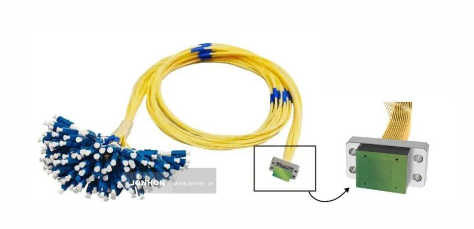
Product Picture:
Product Description:
The 2D fiber array assembly, as a key component of OCS optical switching equipment, is used to realize the input and output functions of array optical signals. This assembly integrates a 2D fiber array and a 2D lens array, and achieves stable output and reliable reception of collimated light beams through their precise coupling and alignment.
Product Advantages:
1、High port density: A 13×11 port configuration has been achieved, with custom solutions available to meet customers’ diverse scenario requirements.
2、Customizable fiber spacing: Supports precise customization of array fiber spacing according to customers’ specific needs, adapting to different application scenarios.
3、High-precision fiber positioning: Adopts precision fiber array processing technology to achieve high-precision fiber positioning, with fiber core offset controlled within 1μm.
4、Low transmission loss: Leverages high-precision coupling and alignment technology to ensure efficient optical signal transmission, with insertion loss (IL) ≤ 0.8dB.
5、High stability: The product has passed rigorous mechanical environment tests to ensure reliable optical signal transmission during operation.
Core Application Areas and Scenarios:
Two-dimensional FA fiber array components are primarily deployed in OCS optical switching equipment, delivering data exchange solutions for advanced data centers supporting applications such as artificial intelligence (AI), machine learning (ML), and high-performance computing (HPC). Specific applications include:
- Optical Communications and Data Centers: Core for High-Density Signal Transmission
Adapting to the high-bandwidth demands driven by 5G, AI, and cloud computing, these serve as core components for parallel optical interconnects.
High-Speed Optical Modules: Within 400G/800G/1.6T parallel optical modules, array configurations like 12×1 and 8×2 precisely couple multi-channel optical chips (VCSEL, PD arrays) with external fibers. This enables synchronous transmission and reception of multiple signals, boosting transmission rates.
Data Center Interconnect: Aligns with short-distance high-speed interconnect needs between servers and switches in “leaf-spine” architectures. High-density characteristics reduce component size, meeting requirements for “low power consumption, compact dimensions, and high integration.”
Backbone Network Expansion: Combined with WDM devices in OXC equipment, enables centralized scheduling and distribution of multi-wavelength, multi-channel signals, supporting FTTH and backbone network upgrades.
- Optical Sensing: Multi-Channel Parallel Detection and Imaging
Enables simultaneous multi-target sensing by connecting multiple sensing fibers alongside arrayed light sources/detectors.
Distributed Sensing: Connects tens to hundreds of fibers to distribute light signals and receive echoes, enabling large-scale, multi-point synchronous monitoring for oil/gas pipeline leak detection and bridge/tunnel surveillance.
Biomedical Applications: Serves as an optical signal interface in confocal microscopes and OCT devices to enhance imaging resolution and speed; enables parallel detection of multiple biomarker indicators in immunosensing chips.
Industrial Monitoring: Coupled with multi-channel spectrometers, it synchronously collects spectral signals from different regions of inspected items like semiconductor wafers and food products, enabling high-throughput quality screening.
- Laser Technology: Beam Shaping and Energy Combining
Used for beam arrangement and coupling in high-power laser systems to optimize laser performance.
High-Power Combining: Matrix-arranges dozens of low-power lasers for beam combining, generating high-power lasers suitable for industrial applications like cutting, welding, and 3D printing. Spot shape can be optimized through arrangement patterns.
LiDAR: Connects arrayed emitter units to form a two-dimensional array, expanding the field of view and enhancing ranging efficiency. Combined with receiver arrays, it boosts environmental perception capabilities.
Scientific Systems: Precisely couples and transmits multiple ultra-short pulse lasers or single-photon signals in quantum optics and nuclear fusion research, ensuring experimental stability and precision.
- Semiconductors and Microelectronics: Wafer Inspection and Lithography
Delivers ultra-high alignment accuracy of ≤±0.5μm to meet semiconductor manufacturing demands.
Wafer Defect Detection: Connects arrayed optical probes to simultaneously capture multi-region surface images, achieving 10-100x higher defect identification efficiency than single-channel systems.
Lithography Support: In advanced lithography technologies like EUV, used for optical signal readout after photoresist exposure or laser interferometer signal transmission, ensuring lithography precision.
- Other Emerging Fields
Quantum Communication: Enables parallel transmission and coupling of multi-channel single-photon and other quantum signals in QKD systems, enhancing key distribution rates and security.
AR/VR Display: In high-end AR waveguide array solutions, it interfaces light sources with waveguides, efficiently coupling light signals from micro-LED arrays to optimize display quality.
Application Trends:
As “optical integration” and “parallel processing” become core industry demands, 2D FA components are evolving toward higher channel density (e.g., over 1000 channels), smaller micro-pitch (≤100μm), and co-packaged integration (COB) with optical chips. They will play increasingly critical roles in frontier fields such as 6G communications, quantum computing, and ultra-high-precision manufacturing.


